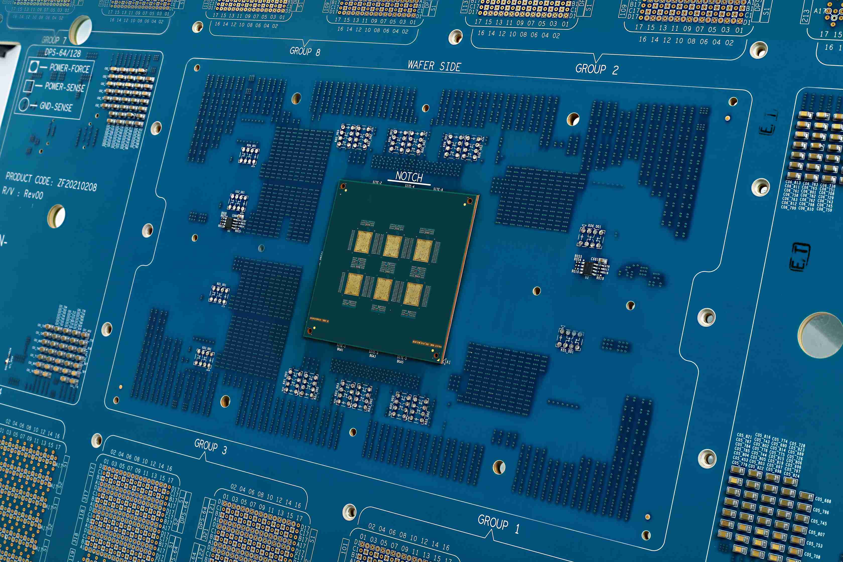
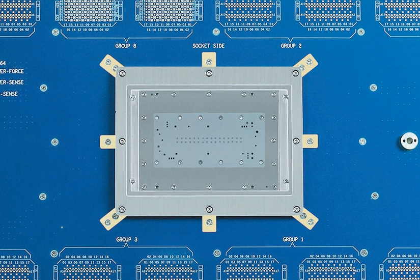
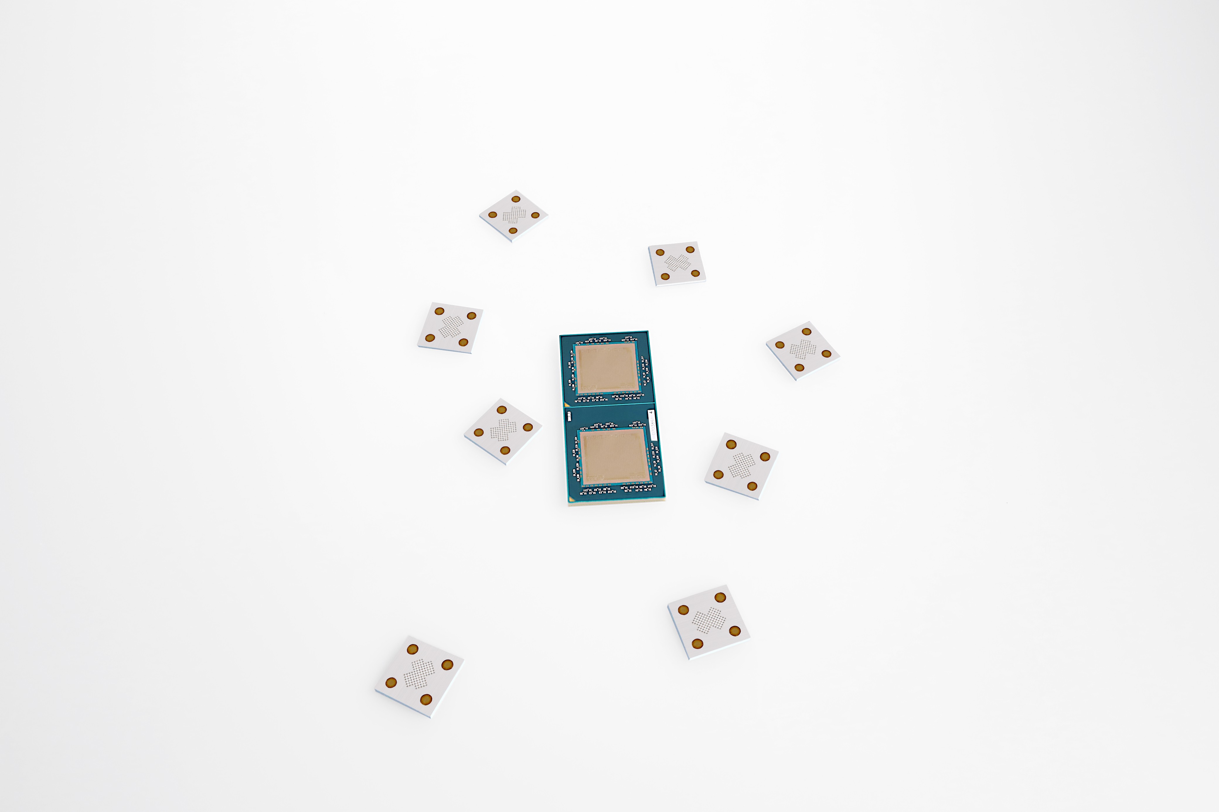
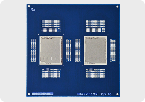
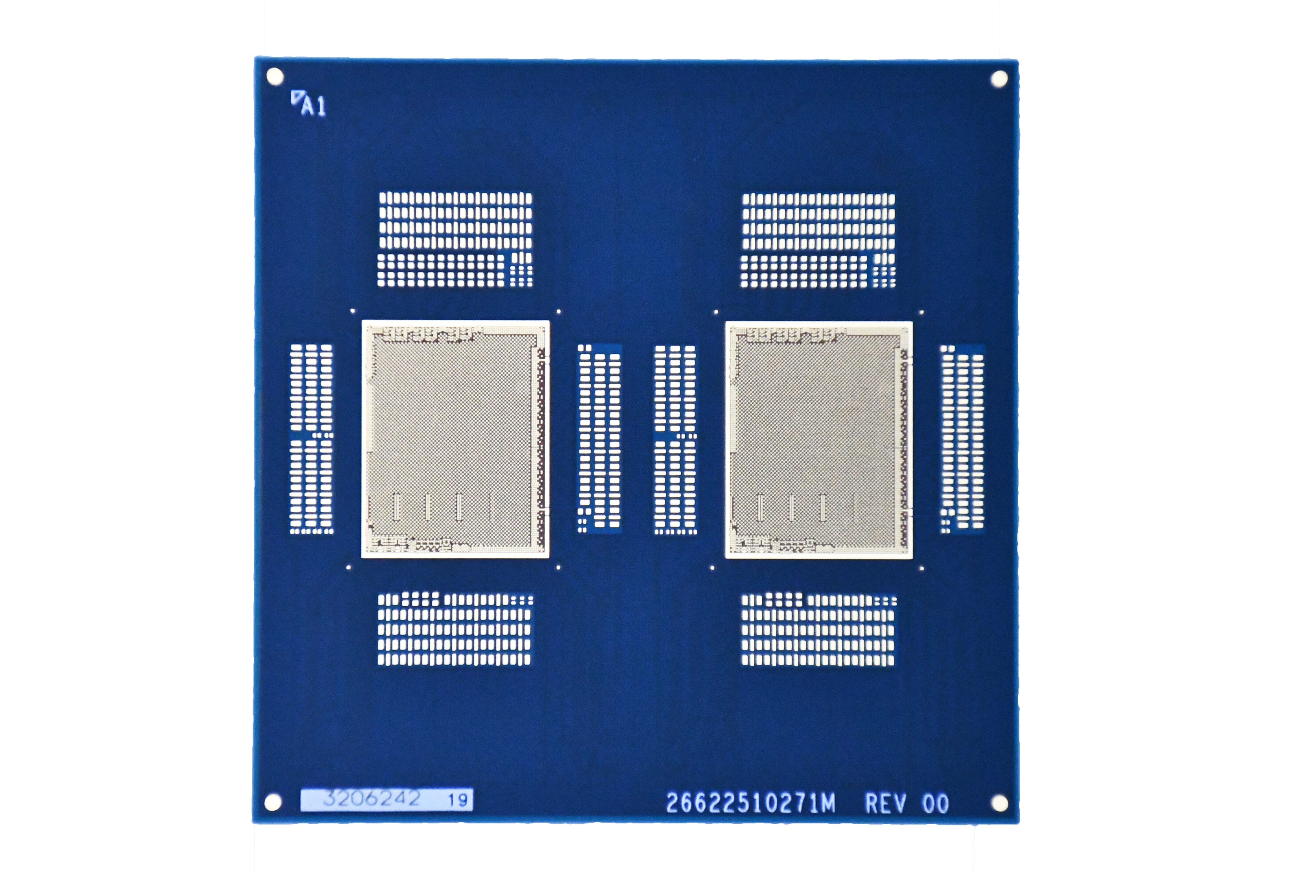
| Probe Card Interposer Specifictions,Top to Bottom |
|---|
| Specification | ZENFOCUS |
| Bump pitch I/O ares or w/b pad pitch | 50um,60um,80um,100um+ |
| Maximum die size or multi-die array size | 100mm X 100mm |
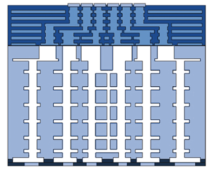
| Type (Interposer) | Organic Build-up with Core & Coreless |
| Material | Normal substrate material |
| # of Build-up layers (per side) | 2~14 (max) |
| # of Core layers | 2~14 (max) |
| Maximum number of separate power leves requiring a plane | depend on Current and Voltage of IC |
| Core via pith | 350um+ |
| Core via diameter | 130um+ |
| Buld-up lines and spaces requirement (include top layer) | 14~20um/14~20um |
| Thickness requirement | 1.0~3.0mm |
| Flatness requirement | < 50um (size 50*50mm or smaller
< 75um (size 50*50mm or smaller |
| Top layer metallurgy (die side) | Hard Gold or ENEPIG (Au thickness>0.30um) |
| Top layer to die contact type | Needle |
| Bottion layer metallurgy (probe card side) | ENIG or ENEPIG |
| Bottion layer to probe card contact type | Solder (Both Pb & free) |
| Maximum life of interposer,both time and touch-downs | N/A |