


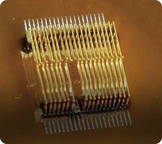
XY positioning accuracy:+/-1μm
Z Positioning accuracy:+/-1μm
Camera resolution:<0.2μm
Pin implanting speed:4000pin/day
Supported Pitch:>50μm
—— Pin implanting
—— Detection


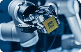
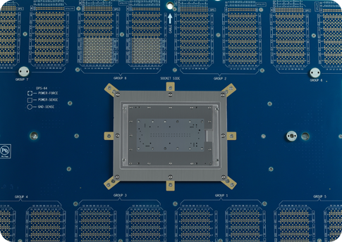
ZENFOCUS has completed the localization of MEMS probe card components of the whole industry chain to realize automated production of probe cards and provide one-stop services from probe card design, simulation, production to testing.

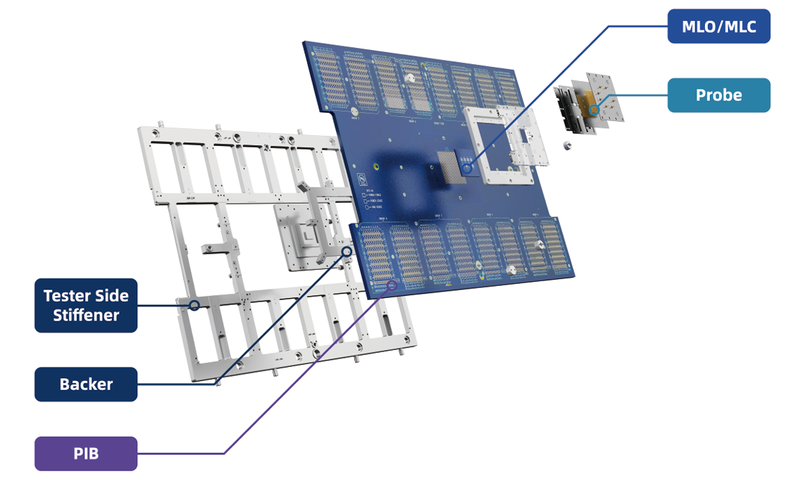
ZENFOCUS has completed localization of Memory probe card components of the whole industry chain to provide one-stop services from probe card design, simulation, production to testing.

ZENFOCUS started the research and development of probe materials and built its production line in 2019, and has completed the development of a number of advanced materials so far. A number of MEMS probes have been adapted to different pitches and CCC, among which 2D MEMS probes have been widely used in the testing of mobile phone processor AP, high-performance computing HPC, intelligent AI and vehicle RF chip products. 3D MEMS probes have been widely used in wafer testing of Nand Flash and DRAM memory products.

The structure design of vertical probe can meet the testing requirements of high density and fine spacing for large-scale BGA array chip, and automatic pin implantation can be realized through automatic equipment, which is efficient and cheap
The multi-component alloy probe material has the advantages of extreme strength and hardness, enabling the fatigue life of the probe pin to exceed 1 million times and reducing the frequency of maintenance of the probe card
The advanced production artistry guarantees the precision of the probe, and makes the probe card have extremely high flatness and test stability
The size and structure of the probe pin tip can be customized to meet the special needs of the chip probe marking and we can cooperate with customers for early marking verification tests
Fully localized probe production reduces the probe design, manufacturing and testing cycle to 10 days and offers customized probes according to customer testing requirements
| Label | ZFCP130MF | ZFBP100MF | ZFBP80MP/F | ZFCP60MF | ZFAP50P/F | ZFBP50P/F |
|---|---|---|---|---|---|---|
| Min.pitch | >130μm | >100μm | >80μm | >60μm | >50μm | >50μm |
| Probe Size | >60μm | >50μm | >45μm | >40μm | >30μm | ~35μm |
| Tip Shape | Flat | Flat | Point Flat | Flat | Point Flat | Point Flat |
Probe | 5.3mm | 5.1mm | 5-6mm | 5.2mm | 5.2mm | 5.1mm |
CCC(Max)@20% | 900mA | 700mA | 500mA | 450mA | 300mA | 350mA |
| Force | ~5gf | ~4gf | ~5-6gf | ~2.2gf | ~1.5-2gf | |
| Material | Customized Alloy | |||||
| Probe type | MEMS | Straight | MEMS | |||
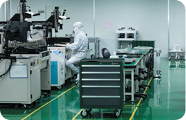
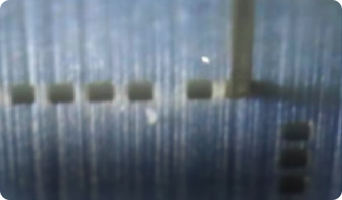
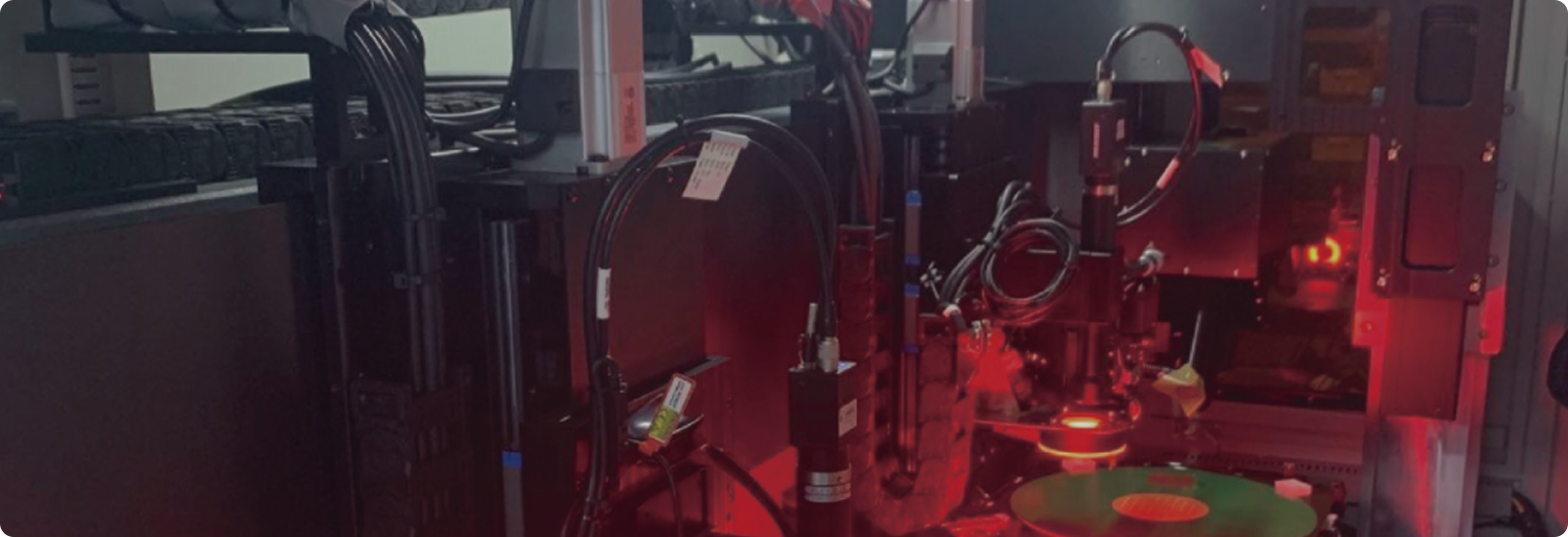
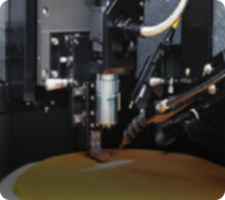
We have realized a variety of automatic pin implanting operation and improved its yield and stability, so that the probe card production is stable and reliable.
XY positioning accuracy:+/-1μm
Z Positioning accuracy:+/-1μm
Camera resolution:<0.2μm
Pin implanting speed:4000pin/day
Supported Pitch:>50μm
| Category | Performance |
|---|---|
| Table size | 200mm*200mm |
| X-axis stroke | -100mm~50mm |
| Y-axis stroke | -50mm~50mm |
| Z-axis stroke | -50mm~50mm |
| Speed | 250mm/s |
| Table load | 10kg |
| Maximum load | 10kg |
| Repetition accuracy | ±0.001mm |
| Category | Performance |
|---|---|
| Positioning stability time | ≤1s |
| Positioning fluctuation | <0.001mm |
| Display resolution | ≤0.0002mm |
| Orthogonality | ≤10 arc sec |
| Category | Performance |
|---|---|
| Speed/pin | 15s |
| Daily production capacity | 4kpin |
| Monthly production capacity | 80kpin |
| Annual production capacity | 900kpin |
The micro-integration technology of the micro-cantilever probe structure enables the probe to have extremely high dimensional accuracy, smaller pin mark slip, and supports the test of small pad.;
The hardness of the probe material is more than 450HV, and the hardness of the tip can reach 600HV after rhodium plating. The contact impedance of the probe is stable, and the wear resistance of the tip is very high.
The probe has high conductivity and supports both high and low temperature tests. The parasitic capacitance is reduced by more than 50% compared with the traditional cantilever probe.
The size and structure of the probe tip can be customized to meet the special needs of the chip probe marking, and we can cooperate with customers for early marking verification test.
| Label | ZFCP130MF | ZFBP100MF | ZFBP80MP/F | ZFCP60MF |
|---|---|---|---|---|
| Min.pitch | >75μm | >75μm | >55μm | >55μm |
| Probe Size | ~15μm | ~15μm | ~10μm | ~10μm |
| Tip Shape | Point | Point | Point | Point |
| Probe Length | 2.93mm | 1.93mm | 2.93mm | 1.93mm |
Probe Length | 1.57mm | 1.57mm | 1.57mm | 1.57mm |
| CCC(Max)@20% Force Off | 1200mA | 1200mA | 800mA | 800mA |
| Probe(gf/mil) | 1.5 | 1.5 | 1 | 1 |
| Material | Customized Alloy | |||
| Probe type | 3D MEMS | |||
Automatic probe welding operation of DRAM large size 3D probe card is realized, taking into account the functions of quality detection and repair after welding, so that the productivity of the probe card is stable and reliable.
XY positioning accuracy:+/-1μm
Z Positioning accuracy:+/-5μm
Camera resolution:<0.2μm
Pin implanting speed:5000pin/day
Supported Pitch:>57μm

| Quantity | Pin Count | Days of pin implantation |
|---|---|---|
| 1 | ≤1s | 20 |
| 2 | <0.001mm | 14 |
| 3 | ≤10 arc sec | 10 |
| Quantity | Pin Count | Days of pin implantation |
|---|---|---|
| 1 | pin welding speed/pin | 12s |
| 2 | Daily production capacity | 5kpin |
| 3 | Monthly production capacity | 100kpin |
| 4 | Annual production capacity | 1000kpin |

Focusing on semiconductor test boards, MEMS probe cards and advanced packaging based on ceramic substrate, ZENFOCUS provides highly competitive high-end products and high-quality services to global integrated circuit chip design companies, packaging and testing plants, and wafer manufacturing plants through independent research and development, production and sales.
![]()