| Time | 2022.H2 | 2023.H1 | 2023.H4 |
|---|---|---|---|
| Wafer | 14nm | 7nm | 5nm |
| LTCC Substate Size | 150*150mm | 200*200mm | 300*300mm |
| LTCC Substate up | 20Layer | 30Layer | >50Layer |
| LTCC Pad Pitch | 250μm | 150μm | 120μm |
| LTCC Line/Space | 100/100um | 50/50μm | 30/50μm |
| LTCC Flantness | <10um | ≤10μm | ≤10μm |
| Thin Film Stack up | 1Layer | 3Layer | 6Layer |
| Thin Film Pad pitch | 85μm | 50μm | 30μm |
| Thin Film Line/Space | 18/25μm | 10/10μm | 5/5μm |
| item | Design Rule (unit : mm) | ||
|---|---|---|---|
| Standard | Advanced | Dev. | |
| (a).Via Hole Dia. | 0.075 | 0.050 | 0.040 |
| (b).Via Cover Dot Dia. | 0.150 | 0.100 | 0.060 |
| (c).Via Pitch | 0.225 | 0.150 | 0.100 |
(d).Via Cover Dot to line Clearance | 0.075 | 0.050 | 0.025 |
| (e).Line Width | 0.075 | 0.050 | 0.020 |
| (f).Line to Line Glearance | 0.075 | 0.050 | 0.020 |
(g).Via Cover DOT Dia. (on Plane) | 0.225 | 0.150 | 0.100 |
(h).Bridge Width(on Plane) | 0.075 | 0.050 | 0.025 |
| (i).Clearance Dia.(on Plane) | 0.2 | 0.2 | 0.1 |
| (j).Via Pitch (on Plane) | 0.25 | 0.25 | 0.15 |
| (k).Ceramic Edge to Patten | 1 | 1 | 1 |
| Tape Thickness* | 0.02~0.2 | 0.02~0.2 | 0.04 |
| item | Design Rule (unit : mm) | |
|---|---|---|
| Standard | Advanced | |
| (a).Thin Film Clearance | 0.025 | 0.015 |
| (b).Thin Film Width | 0.025 | 0.015 |
| (e).Via Hole Dia. | 0.050 | 0.025 |
| (f).Via Cover Dot Dia. | 0.080 | 0.050 |
| (g).C4 Pad Dia | 0.080min | 0.050 |
| (h).C4 Pad Pitch | 0.105min | 0.065 |
| (i1).Polyimide Edge to Pattern | 0.500 | 0.500 |
| (i2).Ceramic Edge to Polyimide Edge | 1 | 1 |
| Probe Card Interposer Specifications,Top to Bottom | |
|---|---|
| Specification | ZENFOCUS |
| Bump pitch I/O ares or w/b pad pitch | 50um,60um,80um,100um+ |
| Maximum die size or multi--die array size | 100mm x 100mm |
| Type (Interposer) | Organic Blulld-up with Core & Coreless |
| Material | Normal substrate material |
| # of Buila-up layers (per side) | 2-14 (max) |
| # of Core layers | 2-14 (max) |
| Maximum number of separate power leVes requlring a plane | depend on Current and Voltage of IC |
| Core via pitch | 350um+ |
| Core via dlameter | 130um+ |
| Build–up lines and spaces requirement (include top layer) | 14~20um/14~10um |
| Thickness requlrement | 1.0~3.0mm |
| Flatness requirement | <50um (size 50*50mm or smaller) <75um (size 50*50mm or larger) |
| Top layer metallurgy (die side) | Hard Gold or ENEPLG (Ay thickness>0.30um) |
| Top layer to die contact type | Needle |
| Bottom layer metallurgy (probe cara side) | ENIG or ENEPLG |
| Bottom layer to probe card contact type | Soder (Both Pb & free) |
| Maximum life of interposer, both time and touch-downs | N/A |

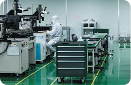
ZENFOCUS focuses on semiconductor test boards, MEMS probe cards and advanced packaging based on ceramic substrate through independent research and development, production and sales
![]()