
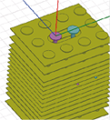
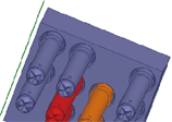
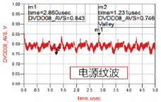
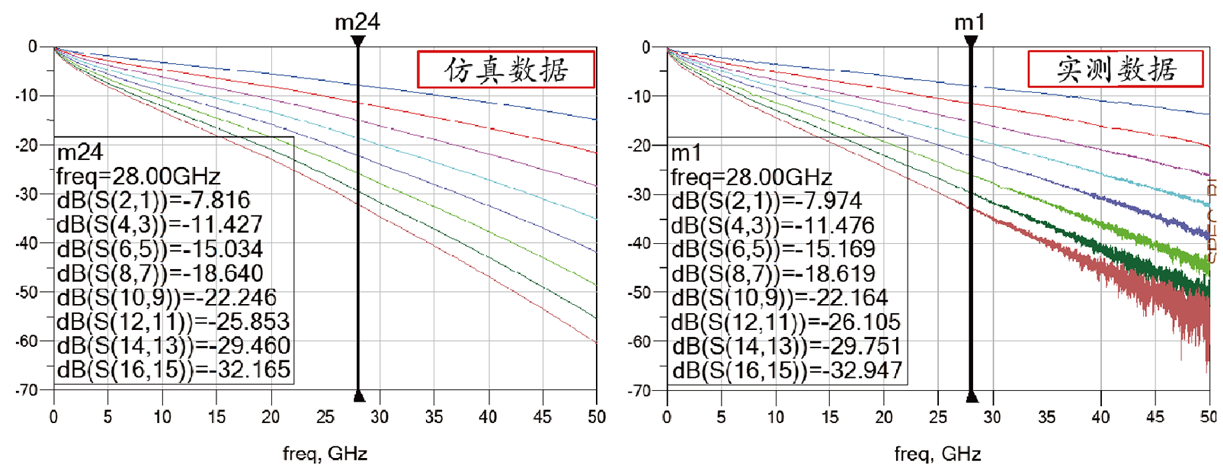
回波损耗在DC-40GHz以内满足规格要求; 插入损耗在目标频率30GHz处,仿真与实 测差异约0.6db。
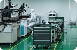
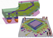
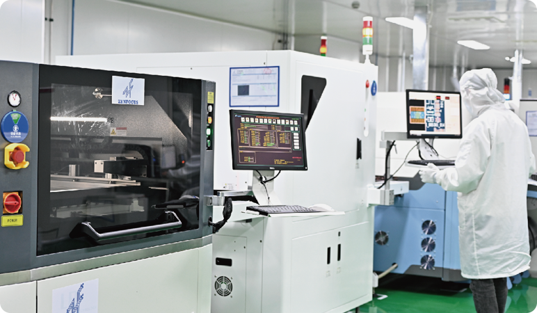
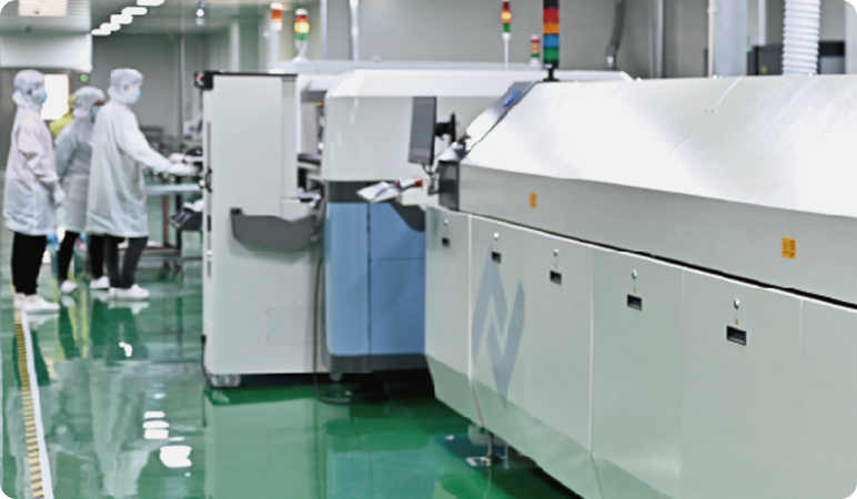
Lingang test board assemblies mass production line
| SMT process capability | Chip area index | ||
|---|---|---|---|
| PCB Size (Max) | 650*610mm | Component size (Max) | 0.15*0.3mm |
| PCB thickness (Max) | 10mm | Chip size (Max) | 100*100mm |
| PCB weight (Max) | 10kg | Chip spacing (Max) | 0.20mm |
| SMT process capability | SMT process capability | ||
|---|---|---|---|
Repetition accuracy
| Temperature uniformity in the warm zone ±2 | Repetition accuracy ±22μm@3Sigma | Repetition accuracy |
Minimum PAD | Oxygen content control <1000ppm | Angle 0.1° | Angle 0.1° |
PAD minimum interval | BGA minimum spacing 0.20mm | Minimum spacing 0.20mm | |
The temperature uniformity in the warm zone is ±2° | |||
| MLC/MLO process capability | Equipment welding capability | ||
|---|---|---|---|
| MLC/MLO size(Max) | 160*160mm | Welding position accuracy | <25μm |
| MLC/MLO dimension weight | ≤500g | Flatness of welding | <65μm |
| MLC/MLO dimension spacing (Min) | 0.25mm | Delivery cycle | 3 days |
| 3D SPI | 3D AOI | 2.5D X-Ray | Flying probe test |
|---|---|---|---|
Repetition accuracy | resolution ≤1μm | Repetition accuracy ±3μm | Detect repeatability ≤10% |
resolution | Detect repeatability ≤10% | Open-circuit test current 2.65A-250mA | |
| Detect repeatability ≤10% | Component size (Max) | Insulation resistance 5MΩ-100MΩ | |
| Open-circuit resistance 0.3Ω-8KΩ |

ZENFOCUS focuses on semiconductor test boards, MEMS probe cards and advanced packaging based on ceramic substrate through independent research and development, production and sales
![]()